Electrical Double Layer based devices, College of Engineering
By A Mystery Man Writer
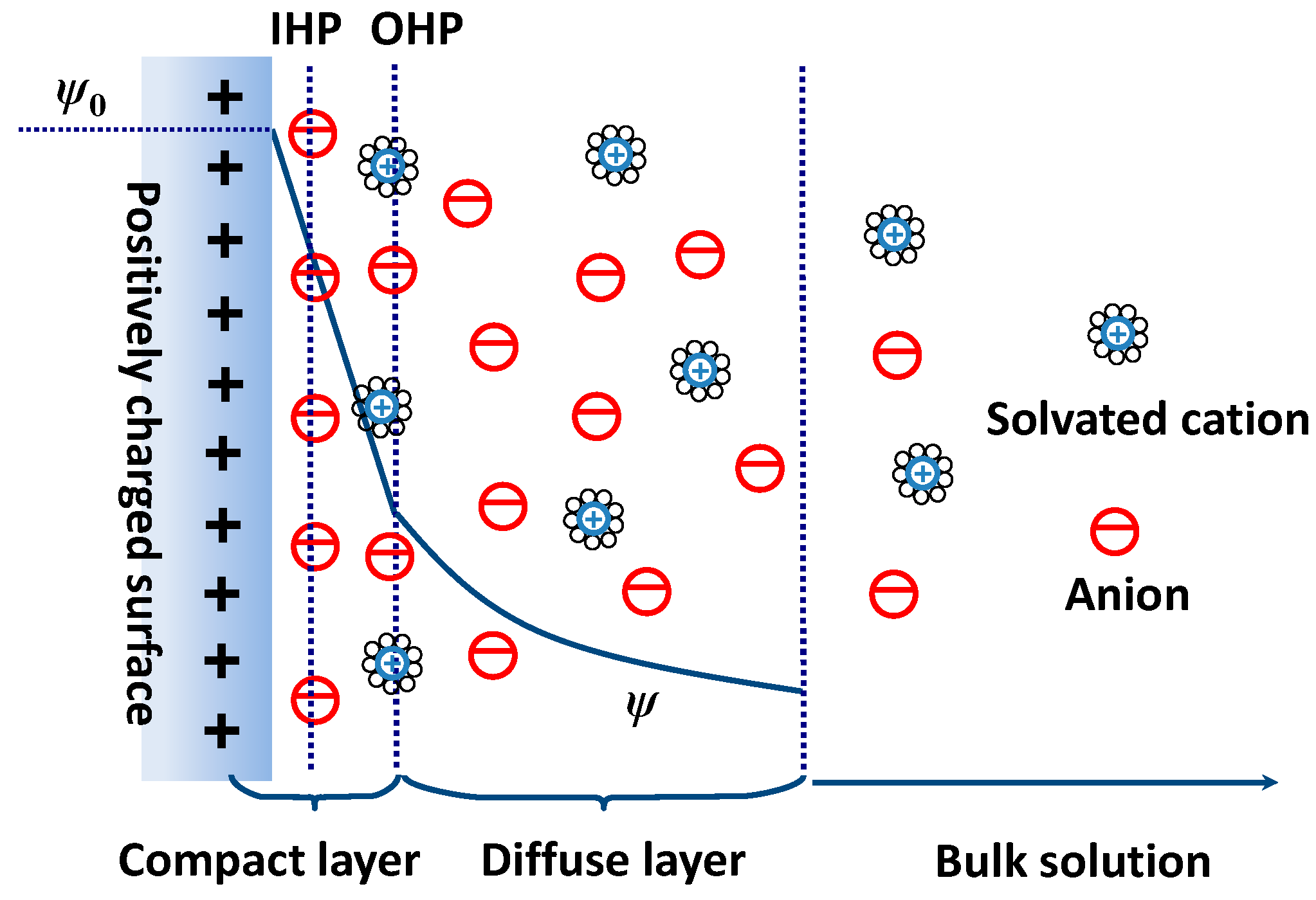
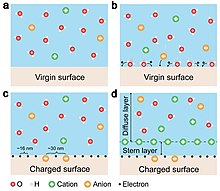
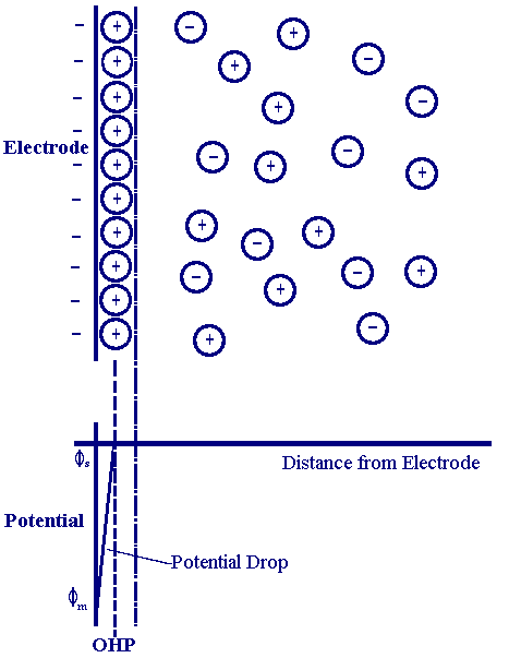
Immersing a metal (electrode) in a salt solution will spontaneously accumulate ions due to image charge to form the well known electrical double layer (EDL). Sign of the charge depends on the Fermi level (i.e., the electrochemical potential) difference between the metal and the solution. For example, gold will accumulate negative ions (i.e., anions). The interfacial structure
Electrical double layer theory

Boosted output performance of triboelectric nanogenerator via electric double layer effect

The electrical double layer solution structure.

Electrical Double Layer Based Devices College Of, 41% OFF
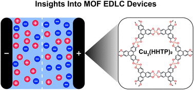
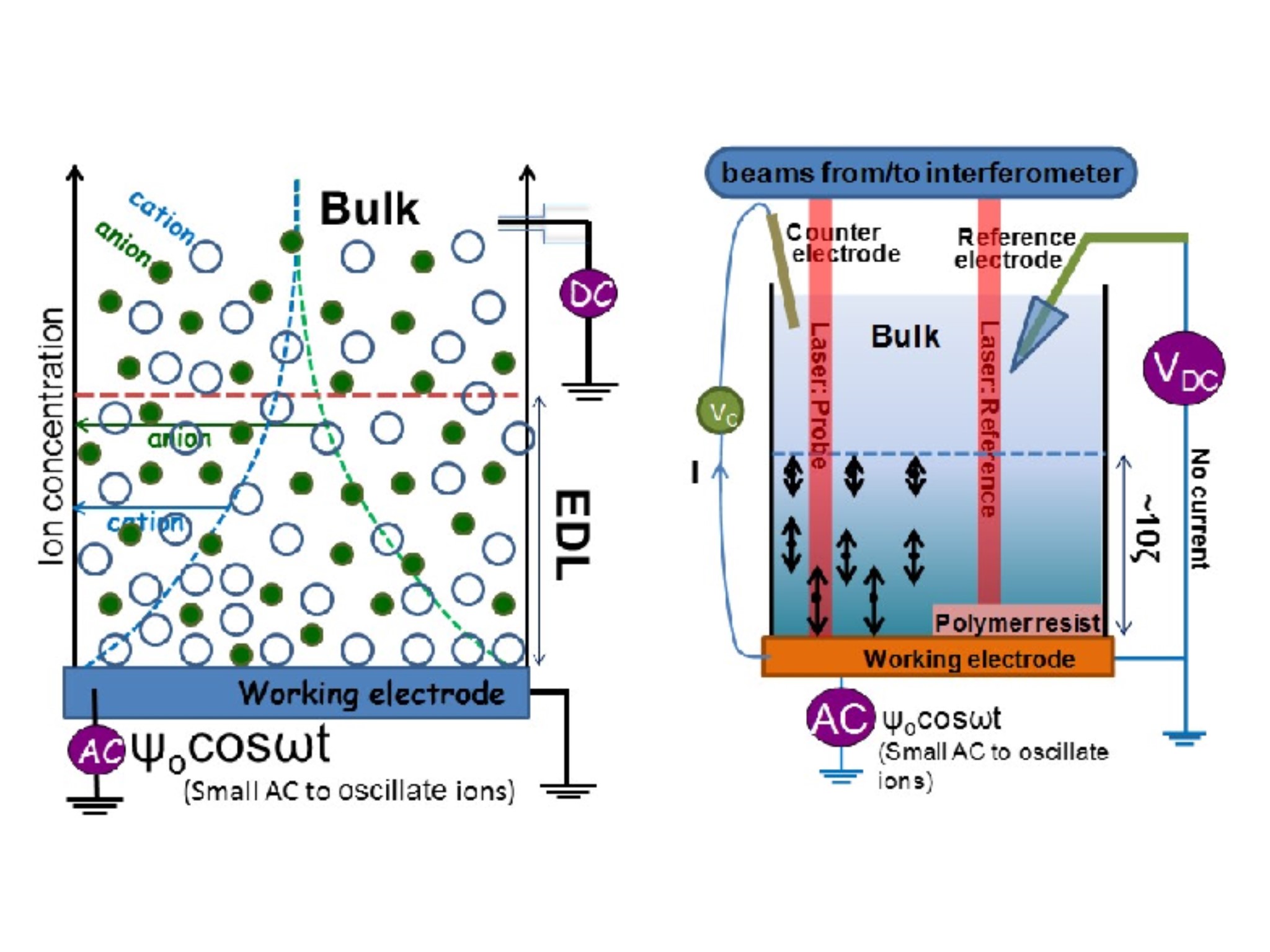
Insights into the electric double-layer capacitance of two-dimensional electrically conductive metal–organic frameworks - Journal of Materials Chemistry A (RSC Publishing)
Fitting Improvement Using a New Electrical Circuit Model for the

Modem vs Router: Understanding Their Roles And Differences
Double layer (surface science) - Wikipedia

Summer Research Experiences for Undergraduates (REU)

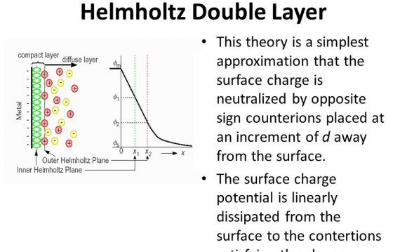
Electric Double Layer - an overview

Publications - Dr. Ali Emadi's Research Group at McMaster University: Canada Excellence Research Chair (CERC) Laureate
Study: Superconductivity switches on and off in “magic-angle” graphene, MIT News

V-One - A Desktop PCB Printer

What is an Electric Double Layer? – Gebbie Lab – UW–Madison
The Electrical Double Layer Department of Chemical Engineering and Biotechnology