What is Collector Base Connection (CB Configuration)? - Definition
By A Mystery Man Writer
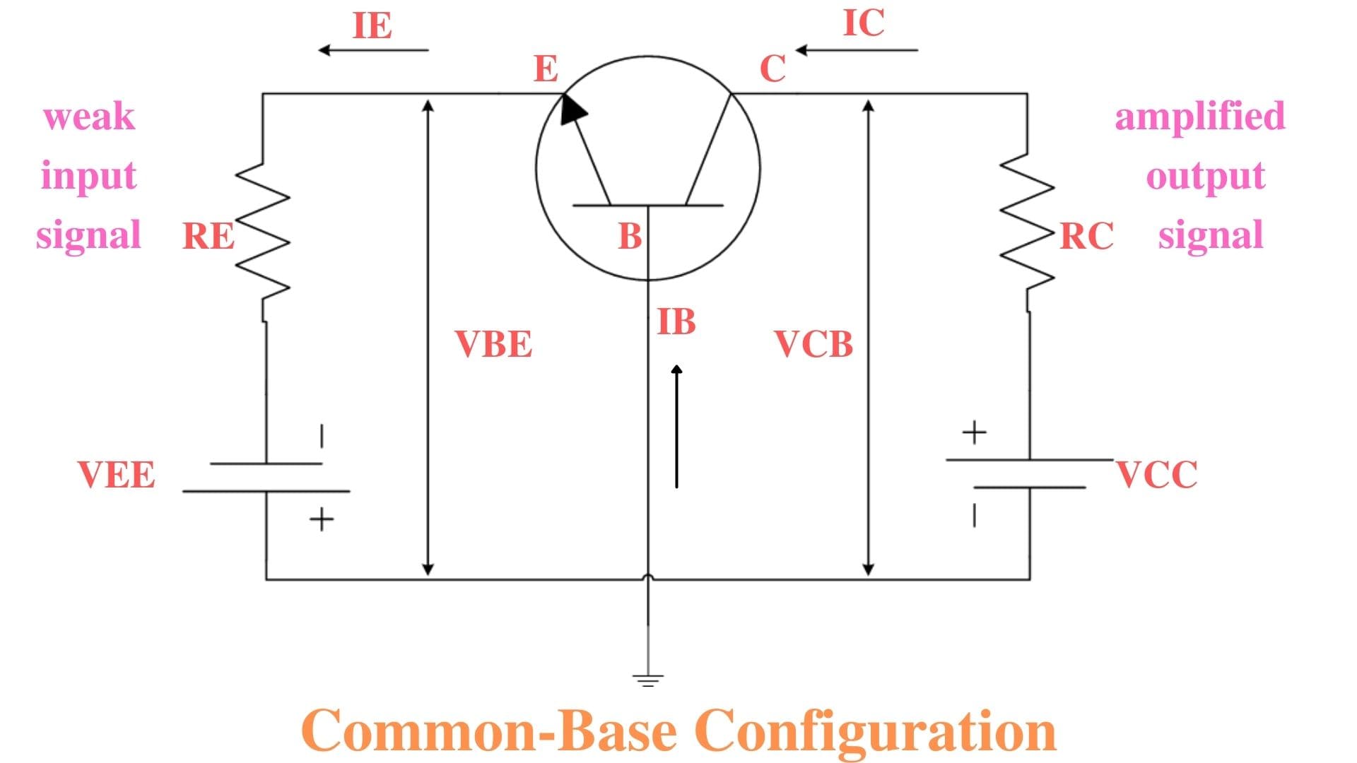
The configuration in which the base of the transistor is common between emitter and collector circuit is called a common base configuration. The common base circuit arrangement for NPN and PNP transistor is shown in the figure below. In common base-emitter connection, the input is connected between emitter and base while the output is taken across collector and base.
What is Common Collector Connection (or CC Configuration

Draw circuit diagram of common base configuration.
Transistor Configuration - Common Base, Collector and Emitter

transistors - How is the Collector-Base region reverse biased in

Uncategorized – Page 8 – Siri's Study Stash
qph.cf2.quoracdn.net/main-qimg-7c0dd0e564b7d215ef8

Circuit Diagram Of Common Base Transistor
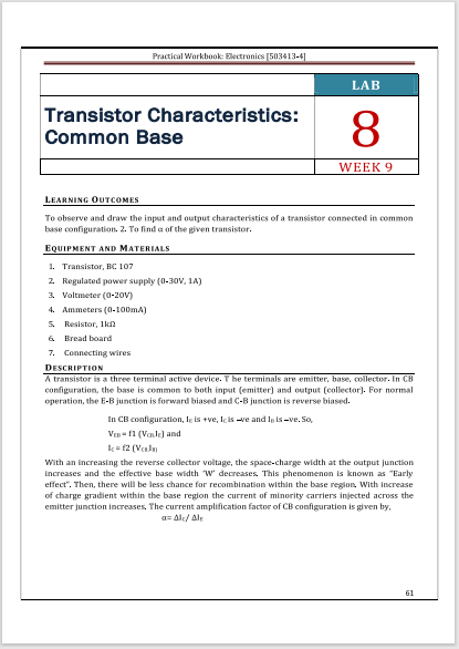
Practical Workbook: ectronics (503413-4, LAB
What is Collector Base Connection (CB Configuration)? - Definition
BJT: Definition, Symbol, Working, Characteristics, Types
BJT Transistors: Symbol, Basics, Construction, Working & Applications

Circuit Diagram Of Common Base Transistor
Fundamentals of CB configuration - MUNDUS 2035

Common Collector Amplifier Tutorial

Common Emitter Amplifier and Transistor Amplifiers


- Pilates Machines for sale in Upper Arlington, Ohio
- The North Face Belay Sun Hooded Shirt - Women's - Clothing

- Good American NEW Large Size 3 Red Sculpt Corset One Piece Swimsuit Swim Beach

- Peonies Flowers Printed Catsuit Blue and Pink Spandex Jumpsuit

- solacol Womens Underwear High Waist High Waist Underwear Women Underwear Women High Waist Womens Large Underwear Medium High Waist Middle-Aged Underwear Women Underwear High Waist