Sunday, Sept 22 2024
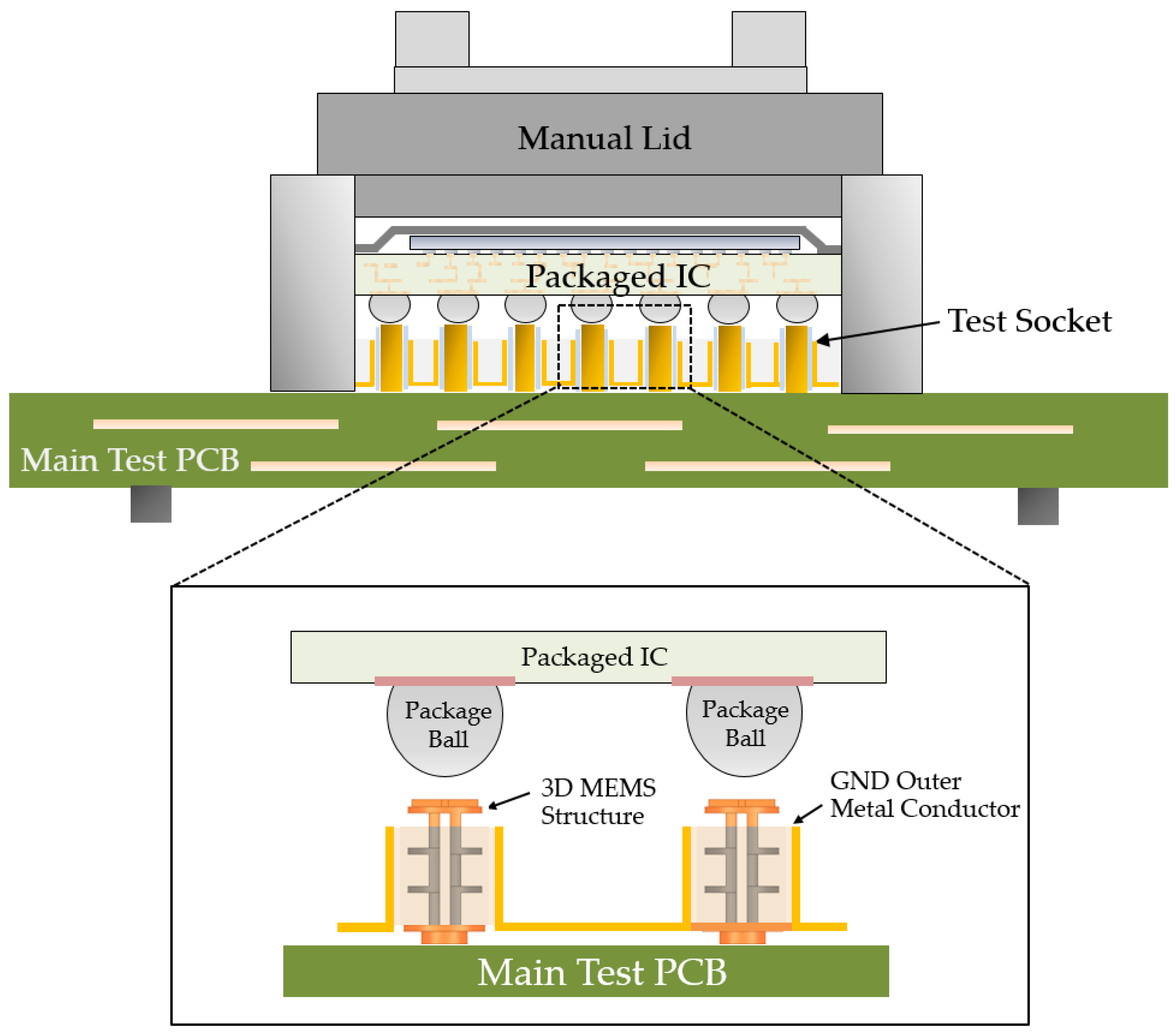
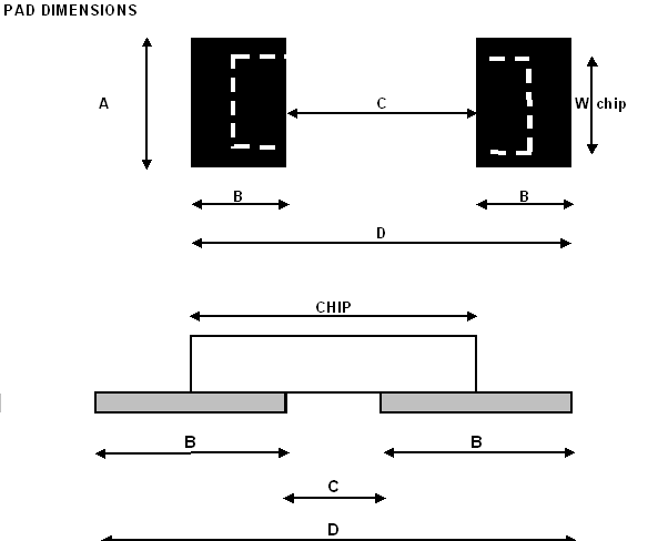
Details of test chip designs: pad pitch, layout, materials, and opening.

By A Mystery Man Writer

Details of test chip designs: pad pitch, layout, materials, and opening.

PCB pad design principles

What is a Pad in PCB Design and Development

Micromachines, Free Full-Text
Sensors, Free Full-Text

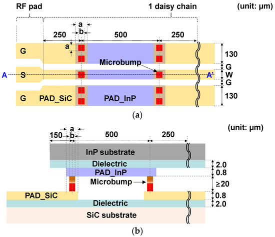
Upper part: Layout of the flip-chip with 60 μm solder spheres applied

The complete guide to PCB pad :types, size, spacing, repair and
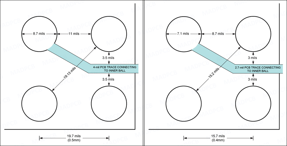
Pitch: SMD Pitch, IC Pitch - PCB Design, Fab & Assembly
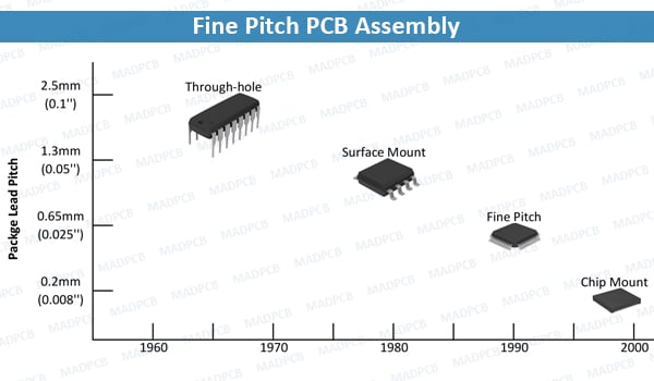
Fine Pitch Technology (FPT): PCB Board Assembly
Chip scale package basics, Advanced PCB Design Blog
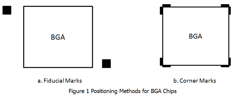
Can't-Miss Layout Tips for BGA Chips

How to Design a BGA? - RAYPCB

Details of test chip designs: pad pitch, layout, materials, and opening.

What is a Pad in PCB Design and Development
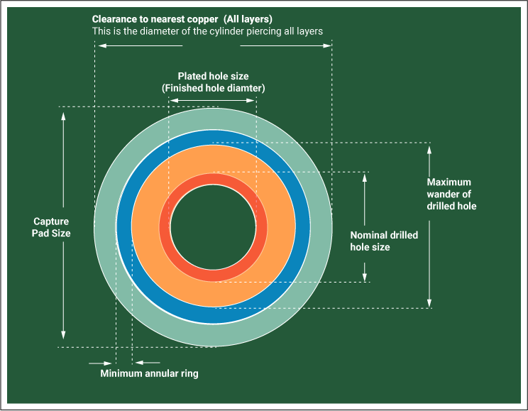
What is a Pad in PCB Design and Development
Related searches


©2016-2024, changhanna.com, Inc. or its affiliates