Wednesday, Sept 25 2024
Schematic of the chip/bump build-up cross-section.
By A Mystery Man Writer

Solder Bump - an overview

Hybrid Bonding Process Flow - Advanced Packaging Part 5

Schematic structures of the cross-section of the indium bump just

Figure 1 from Electrochemical reactions in solder mask of flip

Challenges Grow For Creating Smaller Bumps For Flip Chips

State-Of-The-Art of Advanced Packaging

Materials, Free Full-Text

a Schematic diagram of flip-chip assembly, b flip-chip

Schematic of the chip/bump build-up cross-section.

SEM image of a cross section of an unstressed 30 μm solder bump
Related searches


Related searches
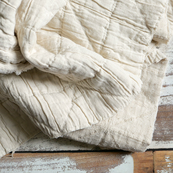
- Un-Dyed Jacquard Quilt Cotton Fabric
- VESTUARIO PROFESIONAL Y UNIFORMES DE DISENO - COCINA - PANTALON BASICO NEGRO - 8540 - DYNEKE

- Amiliashp Women's Spaghetti Strap Tank Top Short Jumpsuit Rompers Bodysuit One Piece Catsuit : Clothing, Shoes & Jewelry

- The Philosophical Society of UPLB - Dr. Lulu Bravo is a Professor Emeritus at the College of Medicine, University of the Philippines Manila. She is the former Vice Chancellor for Research and
- SPANX Stretch Twill Cropped Wide Leg Pant


©2016-2024, changhanna.com, Inc. or its affiliates